 Art & Design
 Auto & Vehicles
 Beauty
 Books & Reference
 Business
 Comics
 Communication
 Dating
 Education
 Entertainment
 Events
 Finance
 Food & Drink
 Health & Fitness
 House & Home
 Libraries & Demo
 Lifestyle
 Maps & Navigation
 Medical
 Music & Audio
 News & Magazines
 Parenting
 Personalization
 Photography
 Productivity
 Shopping
 Social
 Sports
 Tools
Tools
 Travel & Local
 Video Players & Editors
 Weather
 Action
 Adventure
 Arcade
 Board
Board
 Card
Card
 Casino
 Casual
 Educational
 Music
Music
 Puzzle
 Racing
 Role Playing
 Simulation
 Sports
 Strategy
 Trivia
 Word
Word

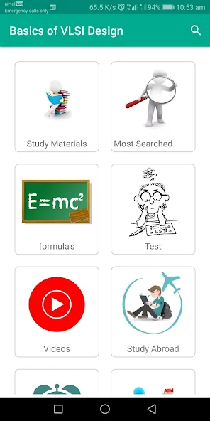


About Basics of VLSI Design
🤞Basics of VLSI Design (Package Name: com.faadooengineers.free_vlsidesign) is developed by Engineering Apps and the latest version of 7 was updated on 2021-04-05. Basics of VLSI Design is in the category of Education. You can check all apps from the developer of Basics of VLSI Design on Android. Currently this app is for free. 🌹 This app can be downloaded on Android Android 4.1+ on ApkDowner or Google Play. All APK/XAPK files on APKDowner.com are original and 100% safe with fast download 😋
The app is a complete free handbook of VLSI with diagrams and graphs. It is part of electronics & communications engineering education which brings important topics, notes, news & blog on the subject. Download the App as quick reference guide & ebook on this electronics & communications engineering subject.
The app covers more than 90 topics of VLSI Design in detail. These topics are divided in 5 units.
You can very easily pass and succeed in your exams or interviews, the app provides quick revision and reference to the topics like a detailed flash card.
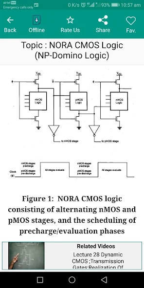
Each topic is complete with diagrams, equations and other forms of graphical representations for easy understanding. Some of topics Covered in this application are:
1. Semiconductor memories :Introduction and types
2. Read Only Memory (ROM)
3. Three transistor DRAM cell
4. One transistor DRAM Cell
5. Flash memory
6. Low - Power CMOS Logic Circuits: Introduction
7. Design of CMOS inverters
8. MOS Inverters : introduction to switching characteristics
9. Scan-Based Techniques
10. Built-In Self Test (BIST) Techniques
11. Historical prospective of VLSI Design : Moore's Law
12. Classification of CMOS digital circuit types
13. A Circuit Design Example
14. VLSI Design methodologies
15. VLSI Design flow
16. Design Hierarchy
17. Concept of regularity, modularity and locality
18. CMOS fabrication
19. Fabrication Process Flow : Basic Steps
20. Fabrication of the nMOS transistor
21. CMOS fabrication : p-well process
22. CMOS fabrication : n-well process
23. CMOS fabrication : twin tub process
24. Stick diagrams and mask layout design
25. MOS transistor : physical structure
26. The MOS System under External Bias
27. Structure and operation of MOSFET
28. The threshold voltage
29. Current voltage characteristics of MOSFET
30. Mosfet scaling
31. Effects of scaling
32. Small Geometry Effects
33. MOS Capacitances
34. MOS inverter
35. Voltage transfer characteristics (VTC) of MOS inverter
36. Inverters with n-type MOSFET load
37. Resistive load inverter
38. Design of Depletion-Load Inverters
39. CMOS inverter
40. Delay time definitions
41. Calculation of Delay Times
42. Inverter Design with Delay Constrains : Example
43. Combinational MOS Logic Circuits : introduction
44. MOS Logic Circuits with Depletion nMOS Loads : Two-Input NOR Gate
45. MOS Logic Circuits with Depletion nMOS Loads : Generalized NOR structure with multiple inputs
46. MOS Logic Circuits with Depletion nMOS Loads : Transient analysis of NOR gate
47. MOS Logic Circuits with Depletion nMOS Loads : Two-Input NAND Gate
48. MOS Logic Circuits with Depletion nMOS Loads : Generalized NAND structure with multiple inputs
49. MOS Logic Circuits with Depletion nMOS Loads : Transient analysis of NAND gate
50. CMOS logic circuits : NOR2 (two input NOR ) gate
51. CMOS NAND2 (two input NAND) gate
52. Layout of Simple CMOS Logic Gates
53. Complex Logic Circuits
54. Complex CMOS Logic Gates
55. Layout of Complex CMOS Logic Gates
56. AOI and OAI Gates
57. Pseudo-nMOS Gates
58. CMOS Full-Adder Circuit & carry ripple adder
59. CMOS Transmission Gates (Pass Gates)
60. Complementary Pass-Transistor Logic (CPL)
61. Sequential MOS logic Circuits : Introduction
62. Behavior of Bistable Elements
63. The SR Latch Circuit
64. Clocked SR Latch
65. Clocked JK Latch
66. Master-Slave Flip-Flop
67. CMOS D-Latch and Edge-Triggered Flip-Flop
68. Dynamic Logic Circuits : Introduction
69. Basic Principles of Pass Transistor Circuits
All topics are not listed because of character limitations set by the Play Store.
The app covers more than 90 topics of VLSI Design in detail. These topics are divided in 5 units.
You can very easily pass and succeed in your exams or interviews, the app provides quick revision and reference to the topics like a detailed flash card.
Each topic is complete with diagrams, equations and other forms of graphical representations for easy understanding. Some of topics Covered in this application are:
1. Semiconductor memories :Introduction and types
2. Read Only Memory (ROM)
3. Three transistor DRAM cell
4. One transistor DRAM Cell
5. Flash memory
6. Low - Power CMOS Logic Circuits: Introduction
7. Design of CMOS inverters
8. MOS Inverters : introduction to switching characteristics
9. Scan-Based Techniques
10. Built-In Self Test (BIST) Techniques
11. Historical prospective of VLSI Design : Moore's Law
12. Classification of CMOS digital circuit types
13. A Circuit Design Example
14. VLSI Design methodologies
15. VLSI Design flow
16. Design Hierarchy
17. Concept of regularity, modularity and locality
18. CMOS fabrication
19. Fabrication Process Flow : Basic Steps
20. Fabrication of the nMOS transistor
21. CMOS fabrication : p-well process
22. CMOS fabrication : n-well process
23. CMOS fabrication : twin tub process
24. Stick diagrams and mask layout design
25. MOS transistor : physical structure
26. The MOS System under External Bias
27. Structure and operation of MOSFET
28. The threshold voltage
29. Current voltage characteristics of MOSFET
30. Mosfet scaling
31. Effects of scaling
32. Small Geometry Effects
33. MOS Capacitances
34. MOS inverter
35. Voltage transfer characteristics (VTC) of MOS inverter
36. Inverters with n-type MOSFET load
37. Resistive load inverter
38. Design of Depletion-Load Inverters
39. CMOS inverter
40. Delay time definitions
41. Calculation of Delay Times
42. Inverter Design with Delay Constrains : Example
43. Combinational MOS Logic Circuits : introduction
44. MOS Logic Circuits with Depletion nMOS Loads : Two-Input NOR Gate
45. MOS Logic Circuits with Depletion nMOS Loads : Generalized NOR structure with multiple inputs
46. MOS Logic Circuits with Depletion nMOS Loads : Transient analysis of NOR gate
47. MOS Logic Circuits with Depletion nMOS Loads : Two-Input NAND Gate
48. MOS Logic Circuits with Depletion nMOS Loads : Generalized NAND structure with multiple inputs
49. MOS Logic Circuits with Depletion nMOS Loads : Transient analysis of NAND gate
50. CMOS logic circuits : NOR2 (two input NOR ) gate
51. CMOS NAND2 (two input NAND) gate
52. Layout of Simple CMOS Logic Gates
53. Complex Logic Circuits
54. Complex CMOS Logic Gates
55. Layout of Complex CMOS Logic Gates
56. AOI and OAI Gates
57. Pseudo-nMOS Gates
58. CMOS Full-Adder Circuit & carry ripple adder
59. CMOS Transmission Gates (Pass Gates)
60. Complementary Pass-Transistor Logic (CPL)
61. Sequential MOS logic Circuits : Introduction
62. Behavior of Bistable Elements
63. The SR Latch Circuit
64. Clocked SR Latch
65. Clocked JK Latch
66. Master-Slave Flip-Flop
67. CMOS D-Latch and Edge-Triggered Flip-Flop
68. Dynamic Logic Circuits : Introduction
69. Basic Principles of Pass Transistor Circuits
All topics are not listed because of character limitations set by the Play Store.
Basics of VLSI Design Update
What's New in the Latest Version 7
Last updated on Apr 5, 2021
Check out New Learning Videos! We have Added
• Chapter and topics made offline access
• New Intuitive Knowledge Test & Score Section
• Search Option with autoprediction to get straight the your topic
• Fast Response Time of Application
• Provide Storage Access for Offline Mode
Install Basics of VLSI Design APK on Android
1.Download Basics of VLSI Design APK For ApkDowner.
2.Tap Basics of VLSI Design.apk.
3.Tap Install.
4.Follow the steps on screen.

 58M+
58M+


 58M+
58M+
 2022-07-11


